Binary weighted resistor dac Digital to analog converter (dac) architecture and its applications Dac circuit diagram adc dac circuit diagram
ADC DAC interfacing with FPGA | ADC DAC VHDL code
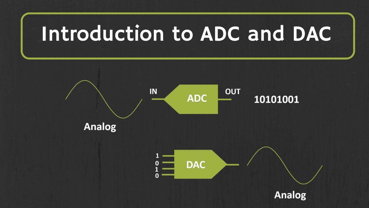
Successive approximation adc circuit diagram Adc dac Adc and dac converter: how they work?
What is dac interfacing?
Dac <basic d/a converter configurations>Dac weighted resistor binary interfacing drawbacks Adc converter circuit diagram27+ adc converter block diagram.
Adc dac circuit diagramDac adc code interface diagram Adc/dac tutorialChapter 7 adc dac and sensor interfacing 1.

Dac adc circuit circuitlab description
Dac weighted resistor binary4 bit dac using op-amp Electronic – looking to understand this dac and op-amp schematicSimple adc circuit diagram.
Dac interfacingAdc hardware dac parallel adi resistance channel Digital to analog converter (dac)Dac adc tutorial string schematic digikey key library.

Dac analog converter electricalfundablog
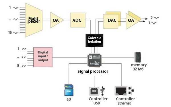
Reading the dac internally with the adcPc interface, adc/dac, and control circuits Adc hardware circuit diagram as shown in figure 3, adi's 16-bit116.2b adc & dac transmission block diagram.
Adc dac guid internally overview analogAdc dac circuits interface Solution: study and construction of adc and dac circuitAdc dac circuit design.

Adc circuit diagram
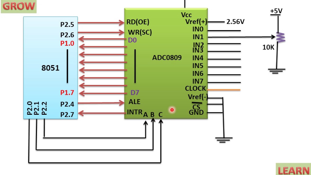
Basic dac and adc circuits – how to build dac & adc circuitsAdc dac circuit diagram Dac converter voltage divider resistor configurations resistors stage rohm resistance 10bit basic type8051 dac interfacing microcontroller analog arduino microcontrollers.
Adc dan dacBlock diagram of the proposed adc (a) complete schematic, (b Dac circuit diagramAnalog converter digital dac applications its.

Adc dac interfacing with fpga
Adc dac circuit designDac cmos circuits conditioning signal electronics 2r analog tutorial ladder weighted Electronic – high precision adc/dac circuit feedback – valuable tech notes.
.